So how I can find this and which ones may I use for it?
Sure, I already read this and the pinout diagram, but I didn’t noticed that fact, that’s why I’m asking that to you, as it seems you have a better knowledge than me about this board or boards in general… I planned to use 36, 39 and 34 to retrieve data from a MICS-6814 sensor (for now, I don’t know how to deal with it when it is not I2C interfaced), and need a way to turn on/off the step up power regulator that powers it, switching a pin on the power regulator from +3,3V to GND.
Unused pins are 0,2,4,12,13,15,16,17,18,23,…
From the ESP32 Technical reference v3.0 p45:
Note that the I/O GPIO pads are 0-19, 21-23, 25-27, 32-39,
while the output GPIOs are 0-19, 21-23, 25-27, 32-33.
GPIO pads 34-39 are input-only.
I had not bumped into this yet and not seen an ESP32 pinout diagram mentioning GPIO 34-39 are input only.
There appears to be no extensive documentation for the ESP32 Arduino Core but you can find documentation for the ESP32 here: Technical Documents | Espressif Systems
I just uploaded a new version of the TTGO v2 pinout diagram: TTGO LoRa32 V2.0 Pinout v2.2.pdf (2.4 MB)
I would expect so, but difficult to say because I have neither the board nor the schematics.
It is common that a diode is placed in series with the USB power (as part of the board design) to prevent current flowing back to the USB port when the board is powered via a 5V / ‘Raw IN’ pin.
You should use a diode in series with the solar panel to prevent current flowing back from the battery when the panel is not producing (enough) energy.
Also take care that the output voltage from the solar panel does not exceed the limits of the voltage regulator on the TTGO board (also when you feed it from the solar panel via the USB port).
Thanks very much. Very clear and useful.
Tonino
You need to add your own pullups too.
Studying the ESP datasheet and technical reference I found no mentioning that GPIO34-GPIO39 cannot have pull-ups or pull-downs. What I did notice is the following:
After a reset input is disabled for the following GPIO ports:
GPIO25, GPIO26, GPIO32, GPIO33, GPIO34, GPIO35, GPIO36, GPIO37, GPIO38 and GPIO39.
(GPIO state can be preserved for low power purposes which can possibly have an effect on this.)
If I am correct input disabled does not implicitly mean that output is enabled (tri-state logic), and pull-ups or pull-downs can only be defined for inputs. So when after reset input for above GPIO ports is disabled so will their pull-ups and pull-downs.
But it may still be possible to (re)enable internal pull-up or pull-down for these GPIO’s when explicitly enabling input for these GPIO’s after a reset. (This is an assumption, I haven’t tested it.)
The requirement for pullups has been reported on the expressif Github as an issue a couple of times at least;
I found much the same, so I have added the external resistors to a board I was designing.
From the ESP32 datasheet;
"GPIO pins 34-39 are input-only. These pins do not feature an output driver or internal pullup/pull-down circuitry. The pin names are: SENSOR_VP (GPIO36), SENSOR_CAPP (GPIO37),
SENSOR_CAPN (GPIO38), SENSOR_VN (GPIO39), VDET_1 (GPIO34), VDET_2 (GPIO35)."
Thanks.
Hi there,
I just wanted to use LMIC with my TTGO32 V2 and I know that for LMIC It’s best to connect:
- HPDIO1 to GPIO33 (mandatory)
- HPDIO2 to GPIO32 (option)
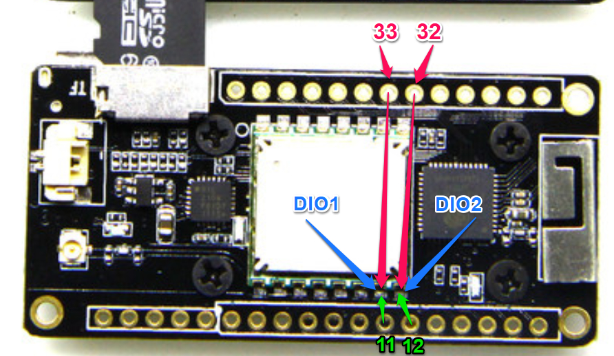
Anyone has a picture of the modification done? may help instead of searching on all the pinout everywehre?
‘Searching on all the pinout everywhere’ ?
How difficult can it be? The pinout is only 8 posts above, and at the top. ![]() Big ESP32 + SX127x topic part 2 - #403 by bluejedi
Big ESP32 + SX127x topic part 2 - #403 by bluejedi
You are free to select any possible free GPIO for connecting DIO1 and DIO2.
But using GPIO33 and GPIO32 keeps it consistent with Heltec and the older TTGO’s so less hassle for looking up differences and modifying configuration settings.
Ok, looks like official way is to link the pink part below

I checked an read back this post, DIO for V2 are already connected to GPIO11/GPIO12 check the green ones, so nothing to do in fact 
Really? ![]()
The long red arrows in your picture have to be manually wired.
On hardware view of course, and it’s easier to change 2 lines of code instead going to heat iron and solder 2 wire ![]()
I checked with my multimeter in continuity mode, looks like they are connected as indicated in green on the picture and that’s strange because schematic does not mention that connection except IO12 connected to SD DAT2.
The board PINS are indeed connected as indicated by the green arrows (DIO1 and DIO2), but the green numbers are nonsense. Those pins are not connected to GPIO11 or GPIO12.
This was already documented in the topic start and in my custom version of the pinout diagram.